

How to develop Sapphire Wafers for quantum - computing applications?
Leave a message

Developing sapphire wafers for quantum - computing applications is a complex yet highly rewarding endeavor. As a sapphire wafer supplier, I have witnessed firsthand the growing demand for these high - quality substrates in the quantum - computing field. In this blog, I will share insights into the process of developing sapphire wafers for quantum - computing applications, from material selection to the final product.

Material Selection
The first step in developing sapphire wafers for quantum - computing applications is selecting the right raw materials. Sapphire, also known as aluminum oxide (Al₂O₃), is a crystalline material with excellent physical and chemical properties. For quantum - computing applications, high - purity sapphire is essential. Impurities in the sapphire can cause interference with quantum states, leading to errors in quantum computations.
We source our sapphire from high - quality mines around the world. The raw sapphire is then carefully inspected to ensure its purity and crystal structure. Advanced analytical techniques, such as X - ray diffraction and Raman spectroscopy, are used to analyze the crystal quality and identify any potential impurities. Only sapphire with the highest purity and optimal crystal structure is selected for further processing.
Crystal Growth
Once the raw sapphire is selected, the next step is crystal growth. There are several methods for growing sapphire crystals, but the most commonly used method for producing sapphire wafers is the Czochralski method. In this method, a small seed crystal is dipped into a molten sapphire solution. As the seed crystal is slowly pulled out of the melt, the sapphire solidifies around the seed, forming a large single - crystal ingot.
The Czochralski method allows for precise control of the crystal growth process. By adjusting the temperature, pulling rate, and rotation speed, we can control the size, shape, and crystal orientation of the sapphire ingot. For quantum - computing applications, the crystal orientation is particularly important. The [100] and [111] orientations are often preferred because they offer better surface flatness and lower defect density, which are crucial for the performance of quantum devices.
Wafer Slicing and Polishing
After the sapphire crystal is grown, it needs to be sliced into thin wafers. A diamond - edged saw is used to cut the sapphire ingot into wafers of the desired thickness. The thickness of the sapphire wafers for quantum - computing applications typically ranges from a few hundred micrometers to a few millimeters, depending on the specific requirements of the quantum device.
Once the wafers are sliced, they are polished to achieve a smooth and flat surface. Polishing is a critical step because any surface roughness or defects can affect the performance of the quantum device. We use a combination of mechanical and chemical polishing techniques to achieve a surface roughness of less than a few nanometers. The polished sapphire wafers are then cleaned to remove any residual polishing agents and contaminants.
Surface Treatment
In addition to polishing, surface treatment is often required to improve the performance of sapphire wafers for quantum - computing applications. One common surface treatment method is passivation. Passivation involves coating the surface of the sapphire wafer with a thin layer of a material that can protect the surface from oxidation and other environmental factors. Silicon dioxide (SiO₂) is a commonly used passivation material because it has good chemical stability and can form a strong bond with the sapphire surface.
Another important surface treatment is doping. Doping involves introducing impurities into the surface layer of the sapphire wafer to modify its electrical and optical properties. For quantum - computing applications, doping can be used to create specific energy levels and quantum states, which are essential for the operation of quantum devices.
Quality Control
Quality control is an essential part of the sapphire wafer development process. We have a comprehensive quality control system in place to ensure that our sapphire wafers meet the highest standards for quantum - computing applications. Every wafer is inspected using a variety of techniques, including optical microscopy, atomic force microscopy, and scanning electron microscopy, to check for surface defects, crystal quality, and thickness uniformity.
In addition to physical inspections, we also perform electrical and optical tests on the sapphire wafers. These tests are used to measure the electrical conductivity, refractive index, and other properties of the wafers. Only wafers that pass all the quality control tests are approved for use in quantum - computing applications.
Applications in Quantum Computing
Sapphire wafers have several important applications in quantum computing. One of the main applications is as a substrate for superconducting qubits. Superconducting qubits are one of the most promising types of qubits for building large - scale quantum computers. Sapphire wafers provide a stable and low - loss substrate for superconducting qubits, which can help to improve the coherence time and performance of the qubits.
Another application of sapphire wafers in quantum computing is in optical quantum systems. Sapphire has excellent optical properties, such as high transparency in the visible and infrared regions, low absorption, and high birefringence. These properties make sapphire wafers ideal for use in optical components, such as waveguides, lenses, and beam splitters, which are essential for optical quantum communication and computation.
Our Product Range
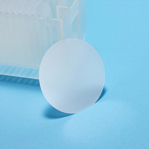
As a sapphire wafer supplier, we offer a wide range of sapphire products for quantum - computing applications. Our Sapphire Wafer is available in various sizes, thicknesses, and crystal orientations to meet the specific requirements of our customers. In addition to sapphire wafers, we also offer Sapphire Light Guide Rod and Sapphire Light Guide Block, which are used in optical quantum systems.
Contact Us for Procurement and洽谈
If you are interested in purchasing sapphire wafers or other sapphire products for your quantum - computing applications, please feel free to contact us. We have a team of experienced professionals who can provide you with detailed product information and technical support. We are committed to providing high - quality products and excellent customer service to meet your needs.
References
- "Quantum Computing: A Gentle Introduction" by Eleanor G. Rieffel and Wolfgang H. Polak.
- "Sapphire: Properties, Growth, and Applications" by John C. Angus and C. Y. Chan.
- "Advanced Semiconductor Materials and Devices" edited by S. M. Sze.


