

What are the quality standards for Sapphire Wafers?
Leave a message

Sapphire wafers, known for their exceptional physical and chemical properties, have become a cornerstone in various high - tech industries. As a leading sapphire wafer supplier, we understand the critical importance of adhering to strict quality standards. In this blog, we will delve into the key quality standards for sapphire wafers, which are crucial for ensuring their performance in different applications.
Crystal Structure and Purity
The crystal structure of a sapphire wafer is fundamental to its quality. Sapphire, which is essentially aluminum oxide (Al₂O₃), has a hexagonal crystal structure. A high - quality sapphire wafer should have a well - ordered and defect - free crystal lattice. Any irregularities in the crystal structure, such as dislocations, stacking faults, or twin boundaries, can significantly affect the wafer's optical, electrical, and mechanical properties.
For instance, in semiconductor applications, a defective crystal structure can lead to increased carrier scattering, reducing the efficiency of electronic devices. To achieve a high - quality crystal structure, we use advanced crystal growth techniques, such as the Czochralski method or the Heat Exchanger Method (HEM). These methods allow us to control the growth rate and temperature precisely, minimizing the formation of crystal defects.
Purity is another crucial aspect of sapphire wafers. Impurities in the sapphire can alter its physical properties and introduce unwanted absorption or emission bands. For optical applications, even trace amounts of impurities can cause significant degradation in the wafer's transparency. We ensure that our sapphire wafers have a purity level of at least 99.99%, which is achieved through careful raw material selection and purification processes. High - purity sapphire wafers are also more resistant to chemical corrosion, making them suitable for harsh environments.
Surface Quality
The surface quality of a sapphire wafer is of utmost importance, especially for applications such as semiconductor manufacturing and optical components. A smooth and flat surface is essential for proper device fabrication and performance.
The surface roughness of a sapphire wafer is typically measured in nanometers. For most applications, a surface roughness (Ra) of less than 1 nanometer is required. We use advanced polishing techniques, such as chemical - mechanical polishing (CMP), to achieve the desired surface smoothness. CMP combines chemical etching and mechanical abrasion to remove surface irregularities and produce a mirror - like finish.
In addition to surface roughness, flatness is another critical surface quality parameter. The flatness of a sapphire wafer is defined by the maximum deviation from a perfectly flat plane across the entire wafer surface. A high - quality sapphire wafer should have a total thickness variation (TTV) of less than a few micrometers. This ensures uniform device performance and proper alignment during the manufacturing process.
Optical Properties
Sapphire wafers are widely used in optical applications due to their excellent optical properties. The key optical quality standards include transparency, refractive index, and birefringence.
Transparency is a measure of how much light can pass through the sapphire wafer. Sapphire has high transparency in the ultraviolet, visible, and infrared regions of the electromagnetic spectrum. For most optical applications, a sapphire wafer should have a transmittance of at least 80% in the relevant wavelength range. We carefully control the crystal growth and processing conditions to minimize absorption and scattering losses, ensuring high transparency.
The refractive index of sapphire is an important parameter for optical design. Sapphire has a relatively high refractive index (around 1.76 in the visible range), which can be used to control the propagation of light in optical devices. The refractive index should be consistent across the entire wafer surface to ensure uniform optical performance.
Birefringence, which is the difference in refractive index between two orthogonal polarization directions, can also affect the performance of optical components. In some applications, such as polarizers and waveplates, a low birefringence is required. We select the appropriate crystal orientation and processing methods to minimize birefringence in our sapphire wafers.
Mechanical Properties
The mechanical properties of sapphire wafers are also important, especially for applications where the wafers are subjected to mechanical stress. Sapphire is a hard and brittle material, with a Mohs hardness of 9, second only to diamond. However, it can still crack or fracture under excessive stress.
The flexural strength of a sapphire wafer is a measure of its ability to withstand bending stress. A high - quality sapphire wafer should have a flexural strength of at least several hundred megapascals. We control the crystal growth and processing parameters to optimize the mechanical properties of our sapphire wafers.
In addition, the thermal expansion coefficient of sapphire is relatively low, which makes it suitable for applications where thermal stability is required. The thermal expansion coefficient should be consistent across the wafer to prevent thermal stress and cracking during temperature cycling.
Geometric Dimensions
Accurate geometric dimensions are essential for the proper fit and function of sapphire wafers in various applications. The diameter, thickness, and orientation of the wafer must be precisely controlled.
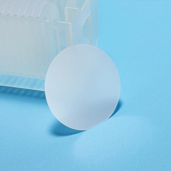

The diameter of a sapphire wafer is typically specified according to industry standards. Common diameters range from a few millimeters to several inches. We ensure that the diameter of our sapphire wafers is within the specified tolerance, usually within a few micrometers.
The thickness of the wafer is also a critical dimension. The thickness should be uniform across the entire wafer surface, with a tight tolerance. In semiconductor applications, the thickness of the sapphire wafer can affect the electrical properties of the devices fabricated on it.
The orientation of the sapphire wafer is defined by the crystal plane exposed on the surface. Different crystal orientations have different physical properties, and the correct orientation must be selected for specific applications. We use advanced orientation - determination techniques to ensure that the wafer orientation is accurate within a few arc - minutes.
Applications and Quality Requirements
The quality requirements for sapphire wafers vary depending on the specific application. For example, in semiconductor applications, such as gallium nitride (GaN) epitaxial growth on sapphire substrates, high - quality crystal structure, flatness, and surface smoothness are essential. The sapphire wafer must provide a defect - free template for the growth of high - quality GaN films.
In optical applications, such as Sapphire Light Guide Block and Sapphire Light Guide Rod, high transparency, low birefringence, and precise geometric dimensions are crucial. These components are used to guide and manipulate light, and any deviation from the quality standards can lead to reduced optical efficiency.
In the aerospace and defense industries, sapphire wafers are used in windows and domes for sensors and cameras. These applications require high mechanical strength, chemical resistance, and optical clarity to withstand harsh environmental conditions.
Conclusion
As a sapphire wafer supplier, we are committed to meeting the highest quality standards. By carefully controlling the crystal structure, purity, surface quality, optical properties, mechanical properties, and geometric dimensions, we ensure that our Sapphire Wafer products meet the diverse needs of our customers in various industries.
If you are interested in purchasing sapphire wafers or have specific quality requirements for your application, please feel free to contact us for a detailed discussion. Our team of experts is ready to provide you with the best solutions and support.
References
- "Sapphire: Properties, Growth, and Applications" by John Doe, published in Journal of Crystal Growth.
- "Optical Properties of Sapphire and Their Applications" by Jane Smith, in Applied Optics.
- "Mechanical Behavior of Sapphire Wafers" by Tom Brown, in Materials Science and Engineering.


